

For the last two years, Gujarat’s semiconductor story has been told almost entirely in concrete and steel — new fabs breaking ground in Sanand, ministers cutting ribbons, crore figures scrolling across news tickers. This week, the state quietly started telling a different story.
On August 8, at the Gujarat Technological University (GTU) campus in Ahmedabad, government officials, professors and industry engineers gathered not to inaugurate a plant, but to plan a Gujarat chip design centre — one meant to teach students how to design the chips those plants will one day manufacture.
It’s a smaller, less photogenic announcement than a $260-million groundbreaking. But if you’re tracking where India’s AI hardware ambitions are actually headed, it might matter more.
What Exactly Got Announced
The Gujarat government’s Department of Science and Technology, acting through the Gujarat State Electronics Mission (GSEM), has proposed a ChipIN Extension Centre and a Centre of Excellence (CoE) for VLSI Design, to be built on the GTU campus in partnership with GTU itself and the Centre for Development of Advanced Computing (C-DAC), the government’s premier applied-computing R&D body.
An orientation programme for the initiative ran over two days starting August 7, with technical sessions covering semiconductor design infrastructure, high-performance computing, indigenous processor ecosystems, IoT solutions and chip development workflows.
Officials say more than 30 engineering institutions from across Gujarat sent representatives — a turnout that, by itself, tells you how much appetite there is among Gujarat’s colleges to get into serious chip work.
The inaugural session was attended by Gujarat’s Department of Science and Technology secretary P. Bharathi, GSEM mission director Neha Kumari, and IIT Gandhinagar director Dr. Rajat Moona, according to officials who briefed PTI.
One detail worth flagging for accuracy: ChipIN itself isn’t a brand-new Gujarat invention. It’s an existing national programme run by the Ministry of Electronics and Information Technology (MeitY) through C-DAC, which already gives select engineering colleges (including some in Karnataka and elsewhere) cloud-based access to chip-design software.
What Gujarat is building is an Extension Centre — essentially a regional hub that will let the state roll this access out to its own engineering colleges in a phased manner, rather than colleges applying individually to the national scheme.
The Real Problem This Is Trying to Solve
Chip design isn’t like writing software. You can’t design even a simple analog circuit or a digital block without Electronic Design Automation (EDA) tools — specialised software made almost exclusively by three global companies: Cadence, Synopsys, and Siemens EDA.
Licences for these tools are notoriously expensive, often running into lakhs of dollars annually, which is exactly why most Indian engineering colleges — even good ones — have historically taught VLSI design as theory on a whiteboard, not as hands-on practice.
The Gujarat chip design centre is meant to close that gap. Through the ChipIN Extension Centre, engineering colleges across the state will get cloud-based, phased access to these EDA platforms, letting students actually design analog circuits, digital chips, phase-locked loops and other components — not just study them.
Industry professionals will also train students and faculty on the full design workflow, because, as one official put it, handing students software tools means little if nobody teaches them how those tools apply to real chip development.
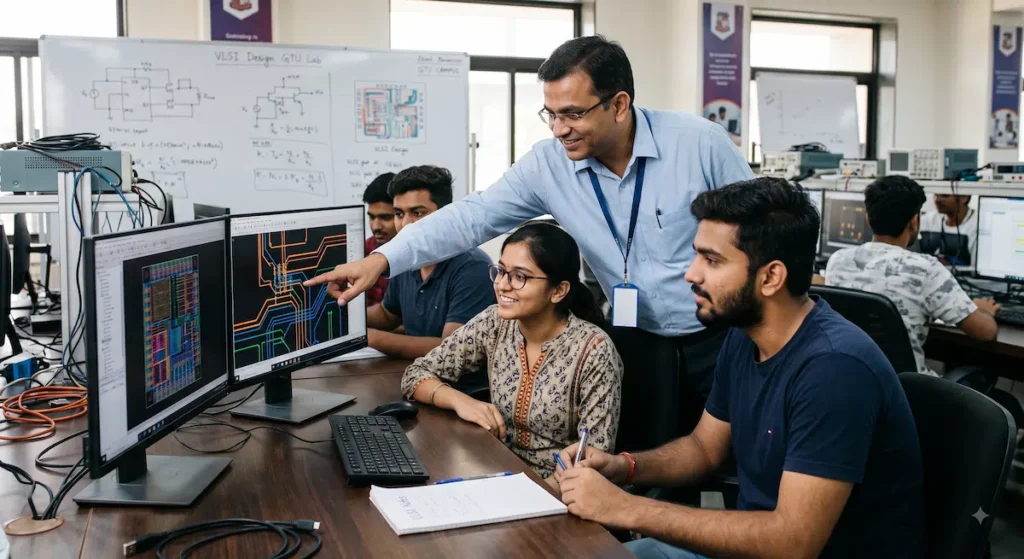
The most interesting part, though, is what happens after a student finishes a design. Under the plan, validated student chip designs will be eligible for fabrication through the Multi-Project Wafer (MPW) route — a shared-fabrication model that lets multiple small, low-volume designs from different institutions ride on the same silicon wafer to split fabrication costs. In plain terms: a Gujarat engineering student could, in theory, see their own chip design turned into an actual physical chip and tested on real hardware — something that almost never happens in a standard four-year electronics degree in India.
Why Gujarat Is Doing This Now
This didn’t happen in a vacuum. Gujarat currently hosts four of India’s ten approved semiconductor manufacturing projects under the India Semiconductor Mission — three in Sanand and one in Dholera, where India’s first full semiconductor fab is targeted for 2028. Three plants are already in commercial production: Micron’s assembly-and-test facility (inaugurated February 2026), Kaynes Semicon’s power-module plant (March 2026), and CG SEMI’s OSAT facility built with Japan’s Renesas Electronics. Kaynes Technology also broke ground on a separate $260-million packaging facility in Sanand just last week.
Speaking at the Viksit Gujarat Summit in GIFT City on August 7 — a day before the ChipIN orientation — Chief Minister Bhupendra Patel said Gujarat was evolving from a manufacturing and renewable-energy hub into a full technology hub, citing the state’s three operational semiconductor plants and its top rank in NITI Aayog’s Investment Friendliness Index, having drawn $73.9 billion in cumulative FDI since 2020.
Put together, the timeline reads like a deliberate two-step plan: first, get the factories built. Now, build the people who can design what goes inside them. This also lines up with the Centre’s own direction — the Union Cabinet approved India Semiconductor Mission 2.0 in mid-July 2026 with a ₹1.27 lakh crore outlay, explicitly widening the mission’s scope beyond fabs to cover chip design, R&D and the broader supply chain. Gujarat’s chip design centre looks very much like a state-level answer to that Centre-level shift.
Why This Matters More Than It Looks
It’s easy to read this as a routine state-government skilling announcement — the kind of story that gets a press release, a PTI wire pickup, and nothing else. But for anyone tracking India’s semiconductor ambitions closely, this fills a gap that’s been widely flagged as India’s weakest link.
India already has real strength in chip design on paper — it’s home to design centres for Qualcomm, Intel, AMD, Nvidia and MediaTek, and roughly a fifth of the world’s semiconductor design engineers reportedly work out of India. But that strength has largely sat inside multinational R&D centres, not homegrown startups or fresh graduates who’ve actually taped out a chip themselves. Manufacturing capacity without a deep local design bench means India risks becoming very good at assembling and packaging chips designed elsewhere — useful, but not the sovereign chip capability the country has publicly said it wants.
A functioning student-to-fabrication pipeline, even a modest one, changes that equation over time. It’s the same logic that’s powered India’s software engineering pipeline for two decades — cheap, structured, hands-on access to real tools, at scale, inside colleges — just applied to silicon instead of code.
The Reality Check
To be fair to your readers, it’s worth being precise about what stage this is at. As of this week, the ChipIN Extension Centre and VLSI CoE are described by officials as a proposal that has completed its orientation phase, not a facility that is operational yet. No public timeline, budget figure, or intake capacity has been disclosed for the centre itself, and it’s not yet clear how many of the 30-plus participating institutions will get access in the first phase versus later ones. This is a foundational step, not a launch — worth watching over the next few months rather than treating as a done deal.
What to Watch Next
- 1 Whether GSEM releases a public timeline and phased rollout list of participating colleges
- 2 Whether the centre announces its first MPW fabrication cycle for student-designed chips
- 3 Whether this becomes a template other semiconductor states — Uttar Pradesh, Odisha, Assam — replicate for their own ChipIN extension centres
- 4 Whether Gujarat-trained VLSI graduates start showing up at Sanand and Dholera’s own facilities, or spin out design startups of their own
Frequently Asked Questions
What is the Gujarat chip design centre?
It’s a proposed ChipIN Extension Centre and Centre of Excellence for VLSI Design, being set up by the Gujarat government’s GSEM in partnership with GTU and C-DAC, to give engineering colleges across the state access to professional chip-design software and training.
What is ChipIN?
ChipIN is an existing national programme run by MeitY through C-DAC that gives select Indian engineering institutions cloud-based access to industry-standard EDA (chip design) tools. Gujarat’s new centre is a state-level extension of this national scheme.
Can students actually get their chip designs manufactured?
Yes — validated student designs are expected to be eligible for the Multi-Project Wafer (MPW) route, which shares fabrication costs across multiple small designs on a single wafer, letting students see their designs become physical, testable chips.
How many semiconductor plants does Gujarat have?
As of August 2026, Gujarat has three operational semiconductor plants (Micron, Kaynes Semicon, and CG SEMI) and hosts four of India’s ten approved semiconductor manufacturing projects overall.
Is this centre already operational?
No. As of this article, it is a proposed facility that has completed an orientation programme; no public launch date, budget, or student intake has been announced yet.
Sources: PTI/Outlook Business (Aug 8, 2026); IANS (Aug 7, 2026); Tele.net.in; India Semiconductor Mission public disclosures. This article will be updated as GSEM releases further details on the ChipIN Extension Centre’s timeline and rollout.